
Design of Ag/TiO2/Ag Composite Nano-Array Structure with Adjustable SERS-Activity

1
College of Materials and Environmental Engineering, Hangzhou Dianzi University, Hangzhou 310018, China
2
The College of Electronics and Information, Hangzhou Dianzi University, Hangzhou 310018, China
3
Shangyu Institute of Science and Engineering, Shaoxing 312000, China
*
Author to whom correspondence should be addressed.
Materials 2022, 15(20), 7311; https://doi.org/10.3390/ma15207311
Submission received: 20 September 2022
/
Revised: 7 October 2022
/
Accepted: 10 October 2022
/
Published: 19 October 2022
(This article belongs to the Special Issue Materials Preparation, Characterization and Applications in Raman Spectroscopy)
Abstract
:How to fabricate large area controllable surface-enhanced Raman scattering (SERS) active nanostructure substrates has always been one of the important issues in the development of nanostructure devices. In this paper, nano-etching technology and magnetron sputtering technology are combined to prepare nanostructure substrate with evolvable structure, and Ag/TiO2/Ag composites are introduced into the evolvable composite structure. The activity of SERS is further enhanced by the combination of TiO2 and Ag and the electron transfer characteristics of TiO2 itself. Deposition, plasma etching, and transfer are carried out on self-assembled 200 nm polystyrene (PS) colloidal sphere arrays. Due to the shadow effect between colloidal spheres and the size of metal particles introduced by deposition, a series of Ag/TiO2/Ag nanostructure arrays with adjustable nanostructure substrates such as nano-cap (NC), nano cap-star (NCS), and nano particle-disk (NPD) can be obtained. These nanoarrays with rough surfaces and different evolutionary structures can uninterruptedly regulate optical plasmon resonance and reconstruct SERS hotspots over a large range, which has potential application value in surface science, chemical detection, nanometer photonics, and so on.
1. Introduction
Surface-enhanced Raman scattering (SERS) has been widely used since it was discovered in 1974 because of its non-destructive, high sensitivity, and high selectivity [1,2]. It has broad and great potential for applications in many fields such as biochemistry [3,4,5], chemical monitoring [5,6], surface science [6], and elucidation of the structural dynamics of molecular transformations [7]. There are many methods available to fabricate SERS substrates with high reproducibility and excellent performance [8,9]. The excellent performance of large area dense Raman signals that can enhance the local surface of the substrate makes these substrates more attractive [10,11]. Since the process of preparing nanostructures will be accompanied by the clusters of metal nanoparticles, these clusters will reduce the density of hot spots and the degree of order of hot spots after a certain period of time, so the enhancement factor (EF) will also decrease [12,13,14]. Therefore, how to fabricate structures with both large-area hot spots and high-density hot spots on SERS substrates is still worthwhile research, and low-cost nanosphere etching (NSE) just needs a little adjustment to meet this requirement [4,6,15]. Many highly ordered nanoarray patterns can be fabricated including periodic nanocaps array [16,17], nanotriangles array [18,19,20], nano dishes array [21,22], nanotubes array, nano rings array [23,24], and nanopillars array [25]. By adjusting the corresponding experimental parameters, more nanogaps can be formed in the above nanostructures [16,17,18,19,20,21,22,23,24,25]. Therefore, it can significantly increase the hot spot density in the nanostructures prepared by NSE technology [18,20].
When deposit metal materials on the colloidal sphere array template by magnetron sputtering, two types of complementary nanostructure arrays are formed on the substrate: one is the NC array formed by the metal film, the other is the hexagonal star array left on the substrate after the template is removed [25,26]. Precious metals with local surface plasmon resonance (LSPR) properties are usually deposited on the template to enhance the local electromagnetic field, while other materials, such as nano-porous GaN [27,28], Si [29,30] and ZnO [30], are also used in this process because of their corresponding properties. TiO2 is often used as an excellent carrier material because of its special optical [31,32] and chemical properties, so it is one of several widely used wide band gap semiconductors [33,34]. In this paper, a simple and efficient method for the preparation of nanostructure arrays is proposed by using the complementary method of plasma etching and magnetron sputtering and three kinds of nanocomposite structures with different hot spots are prepared. On this basis, TiO2 is introduced to further adjust the performance of SERS from the point of view of electron transfer. With the introduction of TiO2, the Raman enhancement factor of SERS reached 4.93 × 10⁵, which is more than twice as much as other similar work [35,36,37,38]. Through the control of the above conditions, the position and distribution of hot spots can be effectively adjusted to significantly increase the density of hot spots.
2. Materials and Methods
2.1. Preparation of Large Area Ordered PS Colloidal Sphere Array
The diameter of polystyrene colloidal sphere is 200 nm, the size deviation is less than 10%, and the solution with a concentration of 10 wt% is purchased from Duke Co (Durham, NC, USA). The deionized water (18.2 MΩ·cm−1) is prepared by a Millipore water purification system. We purchased Ag and TiO2 target (99.99 wt%, Beijing, China) from Beijing TIANRY Science and Technology Developing Center. According to our previous work, dense PS monolayers are prepared by self-assembly method. The wafer is boiled with ammonia, hydrogen peroxide, and deionized water at a volume ratio of 1:2:6 for 20 min to enhance the hydrophilicity of the wafer surface. The 100 μL polystyrene bead solution is mixed with 70 μL anhydrous ethanol by ultrasonic 3 min, the solution is dispersed on the deionized water surface, and then the liquid surface is acted with air. The colloidal spheres are self-assembled to form a dense monolayer, and finally the monolayer is extracted onto the silicon wafer [39].
2.2. Fabrication of the Ag/TiO2/Ag Nano Structural Arrays
Ag and TiO2 films are prepared on PS colloidal sphere array by magnetron sputtering (ATC 1800-F, USA AJA). In the process of thin film deposition, the distance between the PS colloidal sphere array and the target is 20 cm. The bottom pressure of the vacuum chamber is 4.5 × 10⁻⁴ Pa. Working gas is Ar with purity of 99.999% and the pressure is 0.6 pa. The sputtering power of 60 W is applied to the target TiO2, and the sputtering power of 10 W is applied to the target Ag. The Ag NC array peeled off by double-sided tape is then inverted and transferred to another clean silicon wafer. Then, the PS colloid spheres are etched by different times (0 s, 60 s, 120 s, 180 s, and 240 s) with a rate of 1 nm s−1 in a plasma cleaner equipment (RIE–10NR). With the increase of time, the diameter of the colloidal sphere is etched smaller and smaller, but the order of the array does not change. Finally, 5 nm thick TiO2 films and 20 nm Ag films are deposited on the etched PS colloidal microsphere array under the same deposition conditions, i.e., etched after 0 s, 60 s, 120 s, 180 s, and 240 s. With the increase of etching time, the nanostructure gradually evolves from NC to NCS and NPD.
2.3. Characterization of the Nano Structural Arrays
The morphology and microstructure are measured on scanning electron microscope (SEM, 15 kV, JEOL 6500F). Moreover, 4-mercaptobenzoic acid (4-MBA) is purchased from Sigma-Aldrich Co Ltd. X-ray diffraction (XRD is performed on the Rigaku D/MAX 3C X-ray diffractometer with Cu Kα radiation (λ = 1.5418 Å)). The UV-Vis spectrum is obtained by Shimadzu UV-3600 spectrophotometer (Kyoto, Japan). The Raman spectrum is collected on Renishaw Raman with a spectral resolution of 1 cm−1 (London, UK, 2000 confocal microscope spectrometer). The Raman laser wavelength is 785 nm, the power is 500 mw, and the single acquisition time is 1000 ms.
2.4. Finite-Difference Time-Domain (FDTD) Simulations
The electric field distributions of different nanostructure arrays are analyzed using commercial software (Lumerical FDTD solution). During the simulation, the substrate is on the x-y plane, and the simulated nanostructures have corresponding boundary conditions in all three directions of the x, y, and z [40]. The laser of 785 nm is used as the simulated excitation light source, the direction is vertical incidence, and the refractive index of the colloidal sphere is 1.585. The dielectric constant and refractive index of other materials are obtained from the corresponding material database [41]. The geometric parameters of nanostructures are obtained by calculation and SEM images.
3. Results and Discussion
3.1. The Preparation Process of the Ag/TiO2/Ag Nano Structural Arrays
Figure 1 shows the flow chart of the preparation of Ag/TiO2/Ag nanostructure arrays. Firstly, an ordered polystyrene colloidal sphere array (200 nm) is arranged on the silicon wafer (Figure 1A). The method of arranging the colloidal spheres is self-assembly technology, which has been mentioned in previous studies in the group. Then, a layer of Ag film is vertically deposited on the ordered PS colloidal sphere array by magnetron sputtering to form a NC array (Figure 1B). Then, the tightly arranged NC are stripped from the silicon wafer with double-sided tape and inverted and transferred to another silicon wafer (Figure 1C). When the tightly packed NC are completely inverted, some Ag nano bowl (NB) arrays are formed. Then, the PS colloidal spheres in the Ag NB are etched at different times (0 s, 60 s, 120 s, 180 s, and 240 s) to form smaller colloidal spheres. Finally, using the same deposition conditions, 5 nm thick TiO2 films and 20 nm Ag films are deposited successively on the etched PS colloidal sphere array. Several different nanostructure arrays can be obtained by this method (Figure 1D–F).
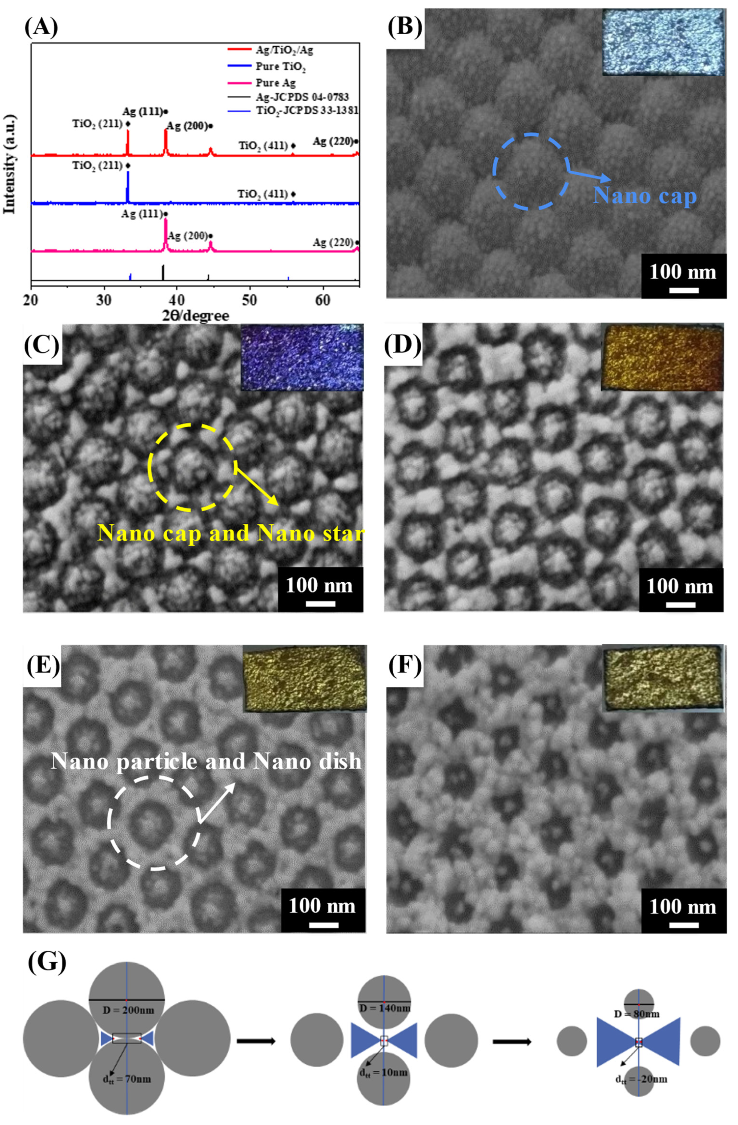
Figure 2 shows the SEM image of the Ag/TiO2/Ag NC array etched after 0 s, 60 s, 120 s, 180 s, and 240 s. With the increase of etching time, the nanostructure gradually evolves from NC to NCS and NPD. Due to the increase of particle size after the introduction of TiO2, different nanostructures are formed under the combined action of particle size and interstitial size. Here, we can calculate the critical value of the process from NCS to nano cap-ring (NCR). From Figure 2G, it can be concluded that when the diameter of colloidal sphere D gradually decreases from 200 nm to 140 nm, the distance between the tips of NCS dtt gradually change from 70 nm to 10 nm, with the further decrease of sphere diameter, which decreases from 140 nm to 80 nm, and the distance between vertices of NCS dtt gradually coincident from 10 nm to −10 nm. These calculated results are the same as the experimental results such as Figure 2B (dtt = 70 ± 5 nm and D = 200 ± 10 nm), Figure 2C (dtt = 10 ± 5 nm and D = 140 ± 10 nm), and Figure 2D (dtt = −10 ± 5 nm and D = 80 ± 10 nm). Figure 2B–F show SEM images of four types of Ag/TiO2/Ag nanostructure arrays. Because the diameter of the etched PS colloidal sphere is different, the reflection color of the array structure on the substrate is also different, as shown in the corresponding optical photo in the figure. For nanostructures with the same diameter and shape, a uniform and consistent reflection color represents a high degree of order on the array. There are two main factors affecting these Ag nanostructure arrays: one is the time of plasma etching, and the other is the particle size of TiO2 deposited by magnetron sputtering. When the etching time is 0 s, there is still a NC array formed by deposition on the substrate. The PS colloidal spheres are closely adjacent to each other, the triangular area between the spheres is too small, and the introduced TiO2 particle size is larger than this region size, so an effective nano-pattern cannot be formed, as shown in Figure 2B. When etching for 60 s, due to the increase of the gap between the spheres, some NCS with an average side length of 95 ± 5 nm appear in the gap region, and because the direct distance between the spheres is still not enough to accommodate the entry of TiO2 particles, so the ring pattern cannot appear, as shown in Figure 2C, the average distance between the tips of the adjacent NCS is dtt = 10 ± 5 nm. When the etching time is further increased to 120 s, due to the further increase of the linear distance between the spheres, TiO2 particles can enter the gap, so the adjacent nano-triangles cover each other, forming the pattern of NCR as Figure 2D show. When etching 180 s, the distance between the colloidal spheres is very large, forming an NPD structure, as shown in Figure 2E. When etching 240 s, as Figure 2F show, the nanostructure has not changed, but the PS colloid sphere is completely etched. XRD patterns in Figure 2A show the existences of Ag and TiO2 in the composite. Ag diffraction peaks at 38.1°, 44.3°, and 64.5° can be assigned to the face-centered cubic crystal structure (111), (200), and (211), in agreement with JCPDS card 04-0783. The diffraction peaks at 33.6° and 51.1° agree with TiO2 (211) and (411) in JCPDS card 33-1381, indicating TiO2 in rutile phase.
3.2. Evaluation of SERS Activity of the Ag/TiO2/Ag Nano Structural Arrays
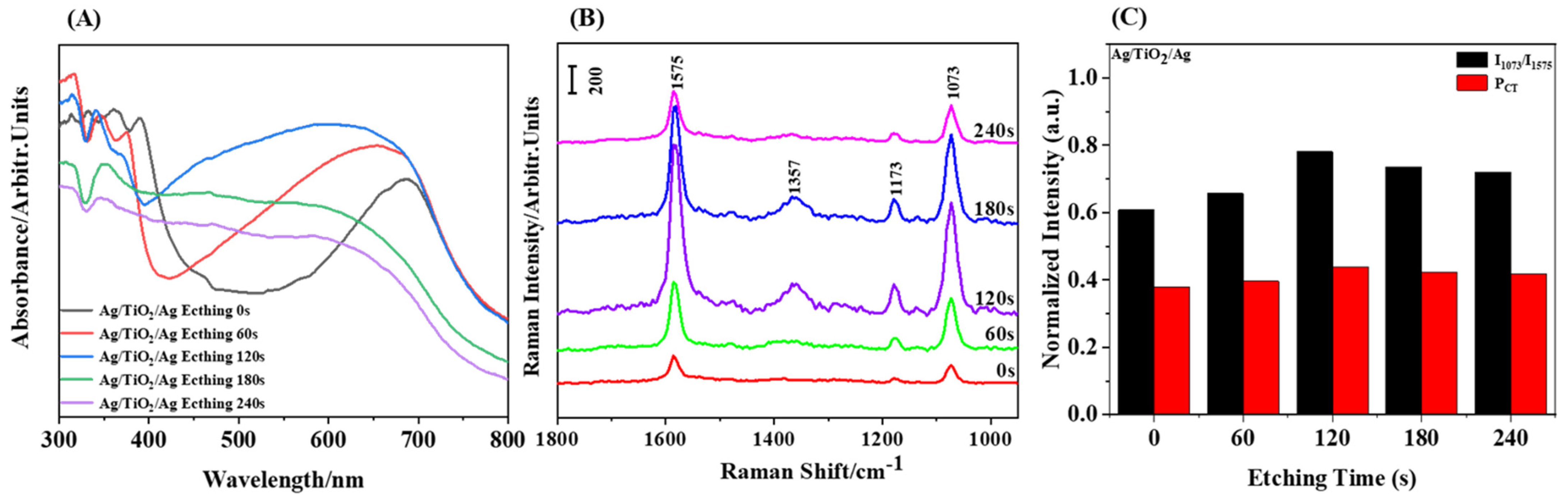
In the UV-Vis spectrum of nanostructures (Figure 3A), different absorption bands can be observed by changing the introduction of different materials. The absorption peak around 300–400 nm is related to the absorption of TiO2-Ag band gap, while the change of absorption peak produced at 400–800 nm can be related to Ag-induced surface plasmon resonance (SPR) [34,42,43]. It can be observed that the absorption peak will blue shift with the change of the structure (Figure 3A), This may be because the Ag and TiO2 binding in the nanostructure reconstructs the Fermi level as the structure changes [44,45,46]. The increase and then decrease of resonance intensity can be attributed to the increase of nano-gap with the increase of etching time from NC to NCS and NPD. The number of hot spots gradually increases, which strengthens the formant due to the surface plasmon, and then with the further prolongation of the etching time, the gap is too large to produce effective hot spots, and the formant gradually weakens. It can be concluded from the first three absorption spectra that the resonance intensity of the NCR is the strongest and the bandwidth is the widest. According to literature reports, this may be due to a lot of electrons from the unique optical properties of TiO2, thus reconstructing a reconstructed Fermi level in the Ag/TiO2/Ag nanostructure [45,46]. In addition, since the interband absorption threshold energy of Ag starts from hv = 3.9 eV, the absorption spectrum shows a sharp increase in the spectral line at 320 nm [43]. By regulating different composite structures, the absorption peak can be adjusted within the 400–800 nm range, which is wider than that of the same type of work [47,48,49].
We choose the 785 nm laser as the excitation light to further verify the conclusion of the resonance intensity of plasmon on the surface of different structures in the absorption spectrum by Raman spectroscopy. As shown in Figure 3B, the SERS spectrum of the Ag/TiO2/Ag nanostructure array, where we use 4-MBA to be SERS probe. There are two strong surface-enhanced Raman scattering peaks that appeared at 1575 cm−1 and 1073 cm−1, corresponding to aromatic ring vibration, respectively, which are used to evaluate the surface-enhanced Raman scattering intensities for different nanostructures. The peak intensities of C-H deformation and COO− stretching vibration modes are weak, which are reflected by 1173 cm−1 and 1357 cm−1, respectively, in Raman spectra [50,51,52]. For Ag/TiO2/Ag nanostructure arrays, the SERS intensity of 4-MBA is positively correlated with etching time; with the increase of the time, the intensity reaches the maximum at 120 s, then decreases gradually, and decreases significantly at 240 s. On the one hand, the intensity of surface-enhanced Raman scattering is affected by the local enhancement of the electromagnetic field caused by the LSPR effect of the precious metal; on the other hand, it is also related to a large number of electron transfer provided by TiO2 in our structure. Therefore, the phenomenon of Raman intensity change can be attributed to the increase of the number and size of nano-gaps with the increase of etching time from 0 s to 120 s, resulting in an increase in hot spot density. At the same time, the increased nano-gap makes it more convenient for TiO2 particles to enter and provide a large number of electrons associated with Ag, resulting in a gradually increased SERS enhancement, but when the etching time continues to increase, the nano-gap size expands beyond the near-field range, so hot spots decrease and the SERS signal decreased. According to the calculation, the EF of different array structures is calculated to be: 5.21 × 10⁴, 1.84 × 10⁵, 4.93 × 10⁵, and 3.12 × 10⁵. Among them, the EF of Ag/TiO2/Ag NC (nano cap-ring) array is the highest, which is slightly higher than that of the same type of SERS substrate.
Since we speculate that the change of SERS signal is due to the interaction between the chemical absorption of 4MBA molecules and nanostructures, the charge transfer (CT) of Ag/TiO2/Ag nanostructures is calculated, and the results are shown in Figure 3C. The degree of charge transfer is calculated by using the 1073 cm−1 (b2) peak belonging to the CCC in-plane bending and C-S stretching combination band (δCCC + vCS) and the 1575 cm−1 (a1) peak belonging to the benzene ring (vCC) [53]. The results show that the relative intensity ratio of the two Raman peaks of 4-MBA has changed significantly. The charge transfer of Ag/TiO2/Ag nanostructures increases at first and then decreases.
According to the theory of CT (ρCT) degree proposed by Lombardi et al., we do the same calculation [54,55]. To quantitatively calculate the relationship between CT resonance and SERS intensity, the ρCT(k) satisfies the following equation:
Here, k is to identify individual molecular lines in the Raman spectrum. Two peaks (1073 cm−1 and 1575 cm−1) are chosen to simplify the calculation. Regarding the 1575 cm−1 (a1), its signal contribution comes entirely from SPR, and its intensity is expressed by , and for this line . The other peak, 1073 cm−1 (b2), is asymmetric, and its strength contribution is not limited to SPR (its intensity is expressed by ) [56]. It represents the intensity part of the SERS intensity contributed by the CT resonance, which is independent of the intensity contributed by the surface plasmon resonance. So, is normally to be zero. Equation (1) can be reduced to as follows:
Figure 3C show the change of relative peak intensities of I1073/I1575 vibrational mode bands. It also reflects the change of CT transition between the lowest empty orbitals (LUMO) of molecules and the Fermi levels reconstructed by different nanostructures [57,58]. The gap between TiO2 nanostructures and Ag nanostructures increases from 0 s to 120 s, which is more beneficial to the mixing and interface diffusion between TiO2 and Ag, so the mixture components of TiO2 and Ag are formed [46]. The special optoelectronic properties of TiO2 make it produce a new Fermi level in the nano structure, which leads to the increase of the transfer degree of a large number of transferable electrons between the structure and 4-MBA molecules, while with the increase of etching time, the nano-gap breaks through a certain size, resulting in Ag can completely cover TiO2, so it is impossible to effectively form composites and play the role of TiO2, so the degree of charge transfer is gradually weakened. The magnitude of CT (ρ CT) reflects the difference between the Fermi level and the molecular LUMO energy level, as well as the matching degree of the excitation energy of the Ag/TiO2/Ag composites, which indicates that the b2 mode of 4-MBA molecule is partially enhanced by CT resonance transition [59].
3.3. Finite-Difference Time-Domain (FDTD) Simulations of the Ag/TiO2/Ag Nano Structural Arrays
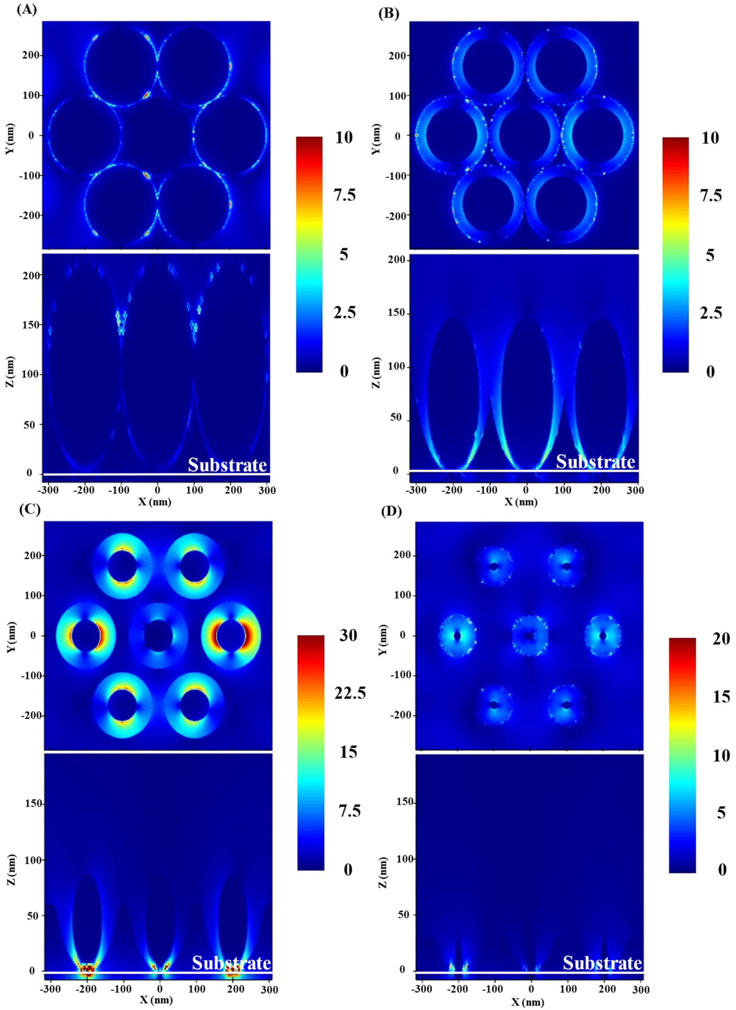
In addition to charge transfer, another important factor affecting the surface enhancement effect of Ag/TiO2/Ag nanostructures is the change of nanostructures. The FDTD numerical simulation method is used to calculate the electromagnetic field around the Ag/TiO2/Ag array composed of NC, NCS, NCR, and NPD, and the influence of different nanostructures on the hot spot intensity is studied. The results show that different morphologies have obvious influence on the distribution of hot spots [56,59,60]. For NC arrays, the hot spot is located in the area between the nearest two NC, as shown in Figure 4A. For the NCS array, because a large number of NCS fill the nano-gap, the hot spot density increases significantly, as shown in Figure 4B. When the structure further evolves and the distance between the NCS is reduced to a certain size to become NCR, the hot spot density further increases, as shown in Figure 4C, when the hot spot density and strength reach the strongest. In the simulated side view of Figure 4C, we can see the enhanced position of the electromagnetic field, which shows that the surface of the Ag NCR is enhanced. Therefore, it can be concluded that the hybrid array of NCR has the highest hot spot density. For the NPD array, the simulation shows that the strong electromagnetic field is only distributed in a small part of the bowl bottom, while the electromagnetic field in other places is very similar. As shown in the figure above and below in Figure 4D, the size of the nano-gap is too large. The sharp decrease of hot spot density leads to relatively weak surface-enhanced Raman scattering signals. The simulation results of the above four types of nanostructure arrays are the same as the experimental data, indicating their feasibility in simulating the distribution of hot spots.
4. Conclusions
In this paper, a simple and efficient preparation method is proposed to prepare large area composite nanostructure arrays with adjustable hot spot intensity distribution and reconfigurable position. At the same time, TiO2 materials with special properties are introduced to further enhance hot spots. By controlling the etching time of PS colloidal spheres in Ag NC, four different nanostructure arrays are prepared: NC, NCS, NCR, and NPD. After the introduction of TiO2, the properties of the four structures are further evaluated, and it is observed that the mixed array of NCR has the strongest SERS signal (etching time is 120 s) and the Raman enhancement factor of SERS reached 4.93 × 10⁵, which is slightly higher than that of the same type of SERS substrate. At the same time, we calculate the charge transfer ability of TiO2 in these structures, and the results are in good agreement with the experimental results. FDTD simulation further shows the source of SERS signal is not only the CT process provided by TiO2. Large area highly ordered and high-density nanostructures can significantly improve the strength and density of surface plasmon hot spots. This work has potential application value in surface science, chemical detection, nanometer photonics, and so on.
Author Contributions
X.Z. and W.X. contributed equally to this work. X.Z.: Conceptualization, Data curation, Funding acquisition, Investigation, Methodology, Resources, and Writing—review and editing. W.X.: Data curation, Investigation, Methodology, Software, and Writing—original draft. X.T.: Investigation and Methodology. J.W.: Funding acquisition, Investigation, and Writing—review and editing. Y.W.: Investigation and Writing—review and editing. All authors have read and agreed to the published version of the manuscript.
Funding
This work is supported by the National Natural Science Foundation of China (Nos. 51901060, funder: Xiaoyu Zhao; Nos. 12004090, funder: Jiahong Wen); the National Natural Science Foundation of Zhejiang Province (Nos. LY21E010004, funder: Xiaoyu Zhao; Nos. LQ21A040009, funder: Jiahong Wen); and the Fundamental Research Funds for the Provincial Universities of Zhejiang (No. GK209907299001–025, funder: Jiahong Wen).
Institutional Review Board Statement
Not applicable.
Informed Consent Statement
Not applicable.
Data Availability Statement
Not applicable.
Conflicts of Interest
The authors declare no conflict of interest.
References
- Fleischmann, M.; Hendra, P.J.; McQuillan, A.J. Raman spectra of pyridine adsorbed at a silver electrode. Chem. Phys. Lett. 1974, 26, 163–166. [Google Scholar] [CrossRef]
- Ikramova, S.B.; Utegulov, Z.N.; Dikhanbayev, K.K.; Gaipov, A.E.; Nemkayeva, R.R.; Yakunin, V.G.; Savinov, V.P.; Timoshenko, V.Y. Surface-Enhanced Raman Scattering from Dye Molecules in Silicon Nanowire Structures Decorated by Gold Nanoparticles. Int. J. Mol. Sci. 2022, 23, 2590. [Google Scholar] [CrossRef] [PubMed]
- Jamieson, L.E.; Asiala, S.M.; Gracie, K.; Faulds, K.; Graham, D. Bioanalytical Measurements Enabled by Surface-Enhanced Raman Scattering (SERS) Probes. Annu. Rev. Anal. Chem. 2017, 10, 415–437. [Google Scholar] [CrossRef] [PubMed] [Green Version]
- Spedalieri, C.; Kneipp, J. Surface enhanced Raman scattering for probing cellular biochemistry. Nanoscale 2022, 14, 5314–5328. [Google Scholar] [CrossRef] [PubMed]
- Wang, Y.; Yan, B.; Chen, L. SERS Tags: Novel Optical Nanoprobes for Bioanalysis. Chem. Rev. 2013, 113, 1391–1428. [Google Scholar] [CrossRef] [PubMed]
- Zhang, X.; Zhang, K.; von Bredow, H.; Metting, C.; Atanasoff, G.; Briber, R.M.; Rabin, O. Remote Chemical Sensing by SERS with Self-Assembly Plasmonic Nanoparticle Arrays on a Fiber. Front. Phys. 2022, 9, 764. [Google Scholar] [CrossRef]
- Yan, W.; Yang, L.; Chen, J.; Wu, Y.; Wang, P.; Li, Z. In Situ Two-Step Photoreduced SERS Materials for On-Chip Single-Molecule Spectroscopy with High Reproducibility. Adv. Mater. 2017, 29, 1702893. [Google Scholar] [CrossRef]
- Guselnikova, O.; Lim, H.; Kim, H.-J.; Kim, S.H.; Gorbunova, A.; Eguchi, M.; Postnikov, P.; Nakanishi, T.; Asahi, T.; Na, J.; et al. New Trends in Nanoarchitectured SERS Substrates: Nanospaces, 2D Materials, and Organic Heterostructures. Small 2022, 18, 2107182. [Google Scholar] [CrossRef]
- Haynes, C.L.; Van Duyne, R.P. Nanosphere Lithography: A Versatile Nanofabrication Tool for Studies of Size-Dependent Nanoparticle Optics. J. Phys. Chem. B 2001, 105, 5599–5611. [Google Scholar] [CrossRef]
- Si, S.; Liang, W.; Sun, Y.; Huang, J.; Ma, W.; Liang, Z.; Bao, Q.; Jiang, L. Facile Fabrication of High-Density Sub-1-nm Gaps from Au Nanoparticle Monolayers as Reproducible SERS Substrates. Adv. Funct. Mater. 2016, 26, 8137–8145. [Google Scholar] [CrossRef]
- Jiao, W.; Chen, C.; You, W.; Zhao, X.; Zhang, J.; Feng, Y.; Wang, P.; Che, R. Hollow Palladium-Gold Nanochains with Periodic Concave Structures as Superior ORR Electrocatalysts and Highly Efficient SERS Substrates. Adv. Energy Mater. 2020, 10, 1904072. [Google Scholar] [CrossRef]
- Guerrini, L.; Graham, D. Molecularly-mediated assemblies of plasmonic nanoparticles for Surface-Enhanced Raman Spectroscopy applications. Chem. Soc. Rev. 2012, 41, 7085–7107. [Google Scholar] [CrossRef] [PubMed]
- Wang, J.; Huang, L.; Zhai, L.; Yuan, L.; Zhao, L.; Zhang, W.; Shan, D.; Hao, A.; Feng, X.; Zhu, J. Hot spots engineering in hierarchical silver nanocap array for surface-enhanced Raman scattering. Appl. Surf. Sci. 2012, 261, 605–609. [Google Scholar] [CrossRef]
- Arbuz, A.; Sultangaziyev, A.; Rapikov, A.; Kunushpayeva, Z.; Bukasov, R. How gap distance between gold nanoparticles in dimers and trimers on metallic and non-metallic SERS substrates can impact signal enhancement. Nanoscale Adv. 2022, 4, 268–280. [Google Scholar] [CrossRef] [PubMed]
- Halas, N.J.; Lal, S.; Chang, W.-S.; Link, S.; Nordlander, P. Plasmons in Strongly Coupled Metallic Nanostructures. Chem. Rev. 2011, 111, 3913–3961. [Google Scholar] [CrossRef]
- Wang, H.; Levin, C.S.; Halas, N.J. Nanosphere Arrays with Controlled Sub-10-nm Gaps as Surface-Enhanced Raman Spectroscopy Substrates. J. Am. Chem. Soc. 2005, 127, 14992–14993. [Google Scholar] [CrossRef]
- Yan, W.-G.; Qi, J.-W.; Li, Z.-B.; Tian, J.-G. Fabrication and Optical Properties of Au-Coated Polystyrene Nanosphere Arrays with Controlled Gaps. Plasmonics 2014, 9, 565–571. [Google Scholar] [CrossRef]
- Lin, W.-C.; Huang, S.-H.; Chen, C.-L.; Chen, C.-C.; Tsai, D.P.; Chiang, H.-P. Controlling SERS intensity by tuning the size and height of a silver nanoparticle array. Appl. Phys. A 2010, 101, 185–189. [Google Scholar] [CrossRef]
- Zrimsek, A.B.; Henry, A.-I.; Van Duyne, R.P. Single Molecule Surface-Enhanced Raman Spectroscopy without Nanogaps. J. Phys. Chem. Lett. 2013, 4, 3206–3210. [Google Scholar] [CrossRef]
- Jiang, S.; Chang, L.; Luo, J.; Zhang, J.; Liu, X.; Lee, C.-Y.; Zhang, W. Fabrication of a honeycomb-like bimetallic SERS substrate for the detection of triphenyltin chloride. Analyst 2021, 146, 6170–6177. [Google Scholar] [CrossRef]
- Gu, X.; Wang, K.; Qiu, J.; Wang, Y.; Tian, S.; He, Z.; Zong, R.; Kraatz, H.-B. Enhanced electrochemical and SERS signals by self-assembled gold microelectrode arrays: A dual readout platform for multiplex immumoassay of tumor biomarkers. Sens. Actuators B Chem. 2021, 334, 129674. [Google Scholar] [CrossRef]
- Zhao, X.; Liu, C.; Yu, J.; Li, Z.; Liu, L.; Li, C.; Xu, S.; Li, W.; Man, B.; Zhang, C. Hydrophobic multiscale cavities for high-performance and self-cleaning surface-enhanced Raman spectroscopy (SERS) sensing. Nanophotonics 2020, 9, 4761–4773. [Google Scholar] [CrossRef]
- Chauvin, A.; Lafuente, M.; Mevellec, J.Y.; Mallada, R.; Humbert, B.; Pina, M.P.; Tessier, P.-Y.; El Mel, A. Lamellar nanoporous gold thin films with tunable porosity for ultrasensitive SERS detection in liquid and gas phase. Nanoscale 2020, 12, 12602–12612. [Google Scholar] [CrossRef] [PubMed]
- Cheng, H.; Dong, X.; Yang, Y.; Feng, Y.; Wang, T.; Tahir, M.A.; Zhang, L.; Fu, H. Au nanoring arrays as surface enhanced Raman spectroscopy substrate for chemical component study of individual atmospheric aerosol particle. J. Environ. Sci. 2021, 100, 11–17. [Google Scholar] [CrossRef] [PubMed]
- Li, Y.; Cai, W.; Duan, G. Ordered Micro/Nanostructured Arrays Based on the Monolayer Colloidal Crystals. Chem. Mater. 2008, 20, 615–624. [Google Scholar] [CrossRef]
- Camden, J.P.; Dieringer, J.A.; Zhao, J.; Van Duyne, R.P. Controlled Plasmonic Nanostructures for Surface-Enhanced Spectroscopy and Sensing. Acc. Chem. Res. 2008, 41, 1653–1661. [Google Scholar] [CrossRef] [Green Version]
- Zhao, S.; Wang, H.; Niu, L.; Xiong, W.; Chen, Y.; Zeng, M.; Yuan, S.; Fu, L. 2D GaN for Highly Reproducible Surface Enhanced Raman Scattering. Small 2021, 17, 2103442. [Google Scholar] [CrossRef]
- Lee, K.H.; Jang, H.; Kim, Y.S.; Lee, C.-H.; Cho, S.H.; Kim, M.; Son, H.; Bae, K.B.; Dao, D.V.; Jung, Y.S.; et al. Synergistic SERS Enhancement in GaN-Ag Hybrid System toward Label-Free and Multiplexed Detection of Antibiotics in Aqueous Solutions. Adv. Sci. 2021, 8, 2100640. [Google Scholar] [CrossRef]
- Karadan, P.; Aggarwal, S.; Anappara, A.A.; Narayana, C.; Barshilia, H.C. Tailored periodic Si nanopillar based architectures as highly sensitive universal SERS biosensing platform. Sens. Actuators B Chem. 2018, 254, 264–271. [Google Scholar] [CrossRef]
- Li, S.; Zhang, N.; Zhang, N.; Lin, D.; Hu, X.; Yang, X. Three-dimensional ordered Ag/ZnO/Si hierarchical nanoflower arrays for spatially uniform and ultrasensitive SERS detection. Sens. Actuators B Chem. 2020, 321, 128519. [Google Scholar] [CrossRef]
- Chuaicham, C.; Sekar, K.; Balakumar, V.; Mittraphab, Y.; Shimizu, K.; Ohtani, B.; Sasaki, K. Fabrication of graphitic carbon nitride/ZnTi-mixed metal oxide heterostructure: Robust photocatalytic decomposition of ciprofloxacin. J. Alloys Compd. 2022, 906, 164294. [Google Scholar] [CrossRef]
- Shanmugam, M.; Augustin, A.; Mohan, S.; Honnappa, B.; Chuaicham, C.; Rajendran, S.; Hoang, T.K.A.; Sasaki, K.; Sekar, K. Conducting polymeric nanocomposites: A review in solar fuel applications. Fuel 2022, 325, 124899. [Google Scholar] [CrossRef]
- Wang, Y.; Liu, J.; Ozaki, Y.; Xu, Z.; Zhao, B. Effect of TiO2 on Altering Direction of Interfacial Charge Transfer in a TiO2-Ag-MPY-FePc System by SERS. Angew. Chem. Int. Ed. 2019, 58, 8172–8176. [Google Scholar] [CrossRef] [PubMed]
- Xu, Y.; Zhang, D.; Lin, J.; Wu, X.; Xu, X.; Akakuru, O.U.; Zhang, H.; Zhang, Z.; Xie, Y.; Wu, A.; et al. Ultrahigh SERS activity of the TiO2@Ag nanostructure leveraged for accurately detecting CTCs in peripheral blood. Biomater. Sci. 2022, 10, 1812–1820. [Google Scholar] [CrossRef]
- Xie, Y. Fabrication of Highly Ordered Ag/TiO2 Nanopore Array as a Self-Cleaning and Recycling SERS Substrate. Aust. J. Chem. 2021, 74, 715–721. [Google Scholar] [CrossRef]
- Xie, Y.; Meng, Y. SERS performance of graphene oxide decorated silver nanoparticle/titania nanotube array. RSC Adv. 2014, 4, 41734–41743. [Google Scholar] [CrossRef]
- Fang, H.; Zhang, C.X.; Liu, L.; Zhao, Y.M.; Xu, H.J. Recyclable three-dimensional Ag nanoparticle-decorated TiO2 nanorod arrays for surface-enhanced Raman scattering. Biosens. Bioelectron. 2015, 64, 434–441. [Google Scholar] [CrossRef]
- Guo, J.; Ding, C.; Gan, W.; Chen, P.; Zhang, M.; Sun, Z. Fabrication of black phosphorous quantum dots and Ag nanoparticles co-sensitized TiO2 nanorod arrays as powerful SERS substrate. J. Alloys Compd. 2022, 918, 165621. [Google Scholar] [CrossRef]
- Zhao, X.; Wen, J.; Li, L.; Wang, Y.; Wang, D.; Chen, L.; Zhang, Y.; Du, Y. Architecture design and applications of nanopatterned arrays based on colloidal lithography. J. Appl. Phys. 2019, 126, 141101. [Google Scholar] [CrossRef]
- Li, D.; Lei, C.; Chen, L.; Tang, Z.; Zhang, S.; Tang, S.; Du, Y. Waveguide plasmon resonance induced enhancement of the magneto-optics in a Ag/Bi:YIG bilayer structure. J. Opt. Soc. Am. B 2015, 32, 2003–2008. [Google Scholar] [CrossRef]
- Saracut, V.; Giloan, M.; Gabor, M.; Astilean, S.; Farcau, C. Polarization-Sensitive Linear Plasmonic Nanostructures via Colloidal Lithography with Uniaxial Colloidal Arrays. ACS Appl. Mater. Interfaces 2013, 5, 1362–1369. [Google Scholar] [CrossRef] [PubMed]
- Yang, L.; Wang, W.; Jiang, H.; Zhang, Q.; Shan, H.; Zhang, M.; Zhu, K.; Lv, J.; He, G.; Sun, Z. Improved SERS performance of single-crystalline TiO2 nanosheet arrays with coexposed {001} and {101} facets decorated with Ag nanoparticles. Sens. Actuators B Chem. 2017, 242, 932–939. [Google Scholar] [CrossRef]
- Guo, J.; Zhang, M.; Yin, Z.; Ding, C.; Chen, P.; Gan, W.; Yu, H.; Sun, Z. Construction of black phosphorus nanosheets and Ag nanoparticles co-sensitized TiO2 nanorod arrays as high-performance SERS substrate and photocatalyst. Appl. Surf. Sci. 2022, 592, 153265. [Google Scholar] [CrossRef]
- Wang, Y.; Yan, C.; Chen, L.; Zhang, Y.; Yang, J. Controllable Charge Transfer in Ag-TiO2 Composite Structure for SERS Application. Nanomaterials 2017, 7, 159. [Google Scholar] [CrossRef]
- Awazu, K.; Fujimaki, M.; Rockstuhl, C.; Tominaga, J.; Murakami, H.; Ohki, Y.; Yoshida, N.; Watanabe, T. A Plasmonic Photocatalyst Consisting of Silver Nanoparticles Embedded in Titanium Dioxide. J. Am. Chem. Soc. 2008, 130, 1676–1680. [Google Scholar] [CrossRef]
- Luna, M.; Barawi, M.; Gómez-Moñivas, S.; Colchero, J.; Rodríguez-Peña, M.; Yang, S.; Zhao, X.; Lu, Y.-H.; Chintala, R.; Reñones, P.; et al. Photoinduced Charge Transfer and Trapping on Single Gold Metal Nanoparticles on TiO2. ACS Appl. Mater. Interfaces 2021, 13, 50531–50538. [Google Scholar] [CrossRef]
- Balzano, V.; Cavaliere, E.; Fanetti, M.; Gardonio, S.; Gavioli, L. The Role of Substrate on Thermal Evolution of Ag/TiO2 Nanogranular Thin Films. Nanomaterials 2021, 11, 2253. [Google Scholar] [CrossRef]
- Viana, M.M.; Mohallem, N.D.S.; Miquita, D.R.; Balzuweit, K.; Silva-Pinto, E. Preparation of amorphous and crystalline Ag/TiO2 nanocomposite thin films. Appl. Surf. Sci. 2013, 265, 130–136. [Google Scholar] [CrossRef]
- Zhang, W.; Liu, Y.; Zhou, D.; Wen, J.; Liang, W.; Yang, F. Photocatalytic activity of Ag nanoparticle-dispersed N-TiO2 nanofilms prepared by magnetron sputtering. RSC Adv. 2015, 5, 57155–57163. [Google Scholar] [CrossRef]
- Jiang, X.; Li, X.; Jia, X.; Li, G.; Wang, X.; Wang, G.; Li, Z.; Yang, L.; Zhao, B. Surface-Enhanced Raman Scattering from Synergistic Contribution of Metal and Semiconductor in TiO2/MBA/Ag(Au) and Ag(Au)/MBA/TiO2 Assemblies. J. Phys. Chem. C 2012, 116, 14650–14655. [Google Scholar] [CrossRef]
- Fujisawa, J.-I.; Kaneko, N.; Hanaya, M. Interfacial Charge-Transfer Transitions in TiO2 Nanoparticles Adsorbed with 4-Mercaptobenzenoic Acid: Carboxy versus Thiol Anchor and Adsorbate-to-TiO2 versus TiO2-to-Adsorbate Charge Transfer. J. Phys. Chem. C 2021, 125, 13534–13541. [Google Scholar] [CrossRef]
- Lin, S.; Guan, H.; Liu, Y.; Huang, S.; Li, J.; Hasi, W.; Xu, Y.; Zou, J.; Dong, B. Binary Plasmonic Assembly Films with Hotspot-Type-Dependent Surface-Enhanced Raman Scattering Properties. ACS Appl. Mater. Interfaces 2021, 13, 53289–53299. [Google Scholar] [CrossRef] [PubMed]
- Huh, H.; Trinh, H.D.; Lee, D.; Yoon, S. How Does a Plasmon-Induced Hot Charge Carrier Break a C–C Bond? ACS Appl. Mater. Interfaces 2019, 11, 24715–24724. [Google Scholar] [CrossRef]
- Lombardi, J.R.; Birke, R.L. A Unified View of Surface-Enhanced Raman Scattering. Acc. Chem. Res. 2009, 42, 734–742. [Google Scholar] [CrossRef] [PubMed] [Green Version]
- Lombardi, J.R.; Birke, R.L. A Unified Approach to Surface-Enhanced Raman Spectroscopy. J. Phys. Chem. C 2008, 112, 5605–5617. [Google Scholar] [CrossRef]
- Wang, Y.; Ji, W.; Sui, H.; Kitahama, Y.; Ruan, W.; Ozaki, Y.; Zhao, B. Exploring the Effect of Intermolecular H-Bonding: A Study on Charge-Transfer Contribution to Surface-Enhanced Raman Scattering of p-Mercaptobenzoic Acid. J. Phys. Chem. C 2014, 118, 10191–10197. [Google Scholar] [CrossRef]
- Chen, T.; Wang, H.; Chen, G.; Wang, Y.; Feng, Y.; Teo, W.S.; Wu, T.; Chen, H. Hotspot-Induced Transformation of Surface-Enhanced Raman Scattering Fingerprints. ACS Nano 2010, 4, 3087–3094. [Google Scholar] [CrossRef]
- Zayak, A.T.; Hu, Y.S.; Choo, H.; Bokor, J.; Cabrini, S.; Schuck, P.J.; Neaton, J.B. Chemical Raman Enhancement of Organic Adsorbates on Metal Surfaces. Phys. Rev. Lett. 2011, 106, 083003. [Google Scholar] [CrossRef] [Green Version]
- Farcau, C.; Astilean, S. Mapping the SERS Efficiency and Hot-Spots Localization on Gold Film over Nanospheres Substrates. J. Phys. Chem. C 2010, 114, 11717–11722. [Google Scholar] [CrossRef]
- Kherbouche, I.; Luo, Y.; Félidj, N.; Mangeney, C. Plasmon-Mediated Surface Functionalization: New Horizons for the Control of Surface Chemistry on the Nanoscale. Chem. Mater. 2020, 32, 5442–5454. [Google Scholar] [CrossRef]
Figure 1.
The schematic of preparation of the Ag/TiO2/Ag nano structural arrays. (A) PS colloid spheres array prepared by self-assembly. (B) Depositing Ag film. (C) Placing upside down PS colloid spheres array. (D–F) Etching PS colloid spheres array for different time and depositing TiO2 and Ag film.

Figure 2.
Characterization of composition and morphology of different structures and schematic diagram of their evolution. (A) XRD diagram of the Ag/TiO2/Ag nano structures, the crystal faces of Ag and TiO2 are marked with different labels respectively. (B–F) The SEM of the Ag/TiO2/Ag nano structural arrays. (B) Etching 0 s. (C) Etching 60 s. (D) Etching 120 s. (E) Etching 180 s. (F) Etching 240 s. (G) The evolution of NCS to NCR.

Figure 3.
The absorption spectra and SERS spectra of structural change sequences after the intro--duction of TiO2. (A) The absorption spectra of Ag/Ag nano structural change sequences. (B) Ag/TiO2/Ag etching 0 s, 60 s, 120 s, 180 s, and 240 s. (C) Relative peak intensity and charge transfer for I1073/I1575 of the Ag/TiO2/Ag nanostructure.

Figure 4.
FDTD simulation results of (A) NC (etched for 0 s). (B) NCS (etched for 60 s). (C) NCR (etched for 120 s). (D) NPD (etched for 180 s). The top and bottom half of each diagram represent the top and side views of the simulation results, respectively.
Figure 4.
FDTD simulation results of (A) NC (etched for 0 s). (B) NCS (etched for 60 s). (C) NCR (etched for 120 s). (D) NPD (etched for 180 s). The top and bottom half of each diagram represent the top and side views of the simulation results, respectively.

Publisher’s Note: MDPI stays neutral with regard to jurisdictional claims in published maps and institutional affiliations. |
© 2022 by the authors. Licensee MDPI, Basel, Switzerland. This article is an open access article distributed under the terms and conditions of the Creative Commons Attribution (CC BY) license (https://creativecommons.org/licenses/by/4.0/).
Share and Cite
MDPI and ACS Style
Zhao, X.; Xu, W.; Tang, X.; Wen, J.; Wang, Y. Design of Ag/TiO2/Ag Composite Nano-Array Structure with Adjustable SERS-Activity. Materials 2022, 15, 7311. https://doi.org/10.3390/ma15207311
AMA Style
Zhao X, Xu W, Tang X, Wen J, Wang Y. Design of Ag/TiO2/Ag Composite Nano-Array Structure with Adjustable SERS-Activity. Materials. 2022; 15(20):7311. https://doi.org/10.3390/ma15207311
Chicago/Turabian StyleZhao, Xiaoyu, Wei Xu, Xiuxia Tang, Jiahong Wen, and Yaxin Wang. 2022. "Design of Ag/TiO2/Ag Composite Nano-Array Structure with Adjustable SERS-Activity" Materials 15, no. 20: 7311. https://doi.org/10.3390/ma15207311
Note that from the first issue of 2016, this journal uses article numbers instead of page numbers. See further details here.